

HDLs and basics of hardware design
Introduction
I am not covering the entire process of silcon design in this tutorial. After a quick intro, we will jump into setting up a HDL simulator and get our hands dirty.
For an embedded engineer, hardware design generally referrs to physical components and printed circuit boards (and breadboards at times). While they form the basics of hardware design, when we move towards designing tiny circuits that pack millions, maybe billions of transistors into a tiny silicon die the size of a pencil head, it becomes obvious that we cannot design them in the conventional way. Here we are talking about the design and development of the components we mount on the PCBs themselves.
The design cycle of an application specific integrated circuit (ASIC) starts off with the description of the circuit itself. While schematic based design entry is a way out, over the years we have perfected advanced tools that can convert the logic description of a circuit into hardware schematics. Since traditional programming languages rely on sequential execution (among many other reasons) we have created a class of languages tailor-made to describe asynchronous and combinatorial logic, and we call them hardware description languages (HDLs).
Verilog and VHDL are the two most commonly used HDLs, and we will be using Verilog here.
Note: A caveat to using a high level language is the tendency for a noob to describe all the hardware logic as “behavioral logic” and leaving it for the tool to synthesize the hardware for it. Take extra care to avoid this mistake.
There are numerous in-depth articles available to wrap your head around the nitty gritties of Verilog and I will not be covering it here. I will however guide you through setting up a free and open-source Verilog simulator to experiment with the concepts. I will also run through the basic concepts that will help us go ahead with HDL based design in the following parts of Fun With FPGAs.
Icarus Verilog
Icarus Verilog (or iverilog) is a free and open sourced Verilog synthesizer and simulator. It runs on Linux as well as windows and is powerful enough to work with complex designs.
Installation of iverilog is quiet straight forward .
In Ubuntu, install it from the official repositories using the following command or compile it from source.
sudo apt-get install iverilog
The windows port for iverilog is available here
iverilog comes with two main tools.
- iverilog : the verilog compiler
- vpp : the simulator
To view simulation output waveform, we will use GTKWave.
Verilog design file
Each design file typically contains a Verilog module. A module is nothing but a basic building block of a design with a set of inputs and outputs. Later on in the design flow, these files will be synthesized into actual hardware blocks.
A typical block for an inverter will look like:
module myInv(A,B);
input wire A;
output wire B;
assign B = !A;
endmodule
This code goes into myInv.v in this sample design.
Breaking it down:
myModule is the name of the module and A and B are the associated signals. Further , we declare that A is the input wire and B is the output wire. Wire means that the signal needs to be driven always and it cannot hold a value on its own . Signals that can hold values are called reg. A signal can be inout as well.
assign keyword is used here to invert the input and assign it to the output.
= is a blocking assignment and all statements assigning using a = will happen sequentially. Non-blocking assignments are denoted using <=. All non-blocking assignments in a block happens in parallel, at the same time.
Testbench
A testbench is written as a seperate file, primarily since it is the “non-synthesizable” portion of the design, and is used to just validate the design. Consequently, it can have implement some “exotic” constraints and gimmicks.
Essentially, a testbench is like a top level module that encapsulates the design, feeds the design with input, and monitor the output. Generally, a test bench will not have any I/O signals.
A sample testbench file (myInv_tb.v) for our ivnerter will look like:
module myModule_tb();
wire out;
reg clock;

initial begin
$dumpfile("inv.vcd");
$dumpvars(0,notGate);

clock=0;
#10
$finish;
end

always begin
#1
clock = !clock;
end

myInv notGate(clock,out);
endmodule
Breaking it down:
As described above, there are no I/O lines for a test bench. However, there is an internal register named clock that will act as an input to myInv and a wire out that will capture the output.
This file illustrates one of the main concepts of HDL design. Unlike sequential programming languages, each block (initial and the “always”) executes in parallel. The designer has to keep this in mind always.
The initial block will execute only once at t=0, whereas the always block is like an infinite loop.
Statements that starts with a $ sign are called tasks and are used by the simulator.
Statements starting with a # are delay statements. Execution will halt in that block for number of time units mentioned after the # sign.
Thus, as per the initial clock will be initialised to 0 at t=0 , and execution will end ($finish) after 10 time units.
As per the always block, clock will be inverted every one time unit.
An important point to note about the always block is that it can drive only reg type data and not wire type data.
Line 19 creates an instance of myInv by the name notGate and assigns clock and out to A and B.
$dumpfile is the task used to open a waveform file named inv to capture the behavior of clock and out during simulation.
The 0 passed as first argument to $dumpvars instructs the simulator to capture all signals of module instance notGate. If a 1 is passed, only the signals named in the argument list will be captured in the output file.
“Synthesis” and Simulation
Execute the below command to synthesize the module and test bench.
iverilog -o myInv.vvp myInv.v myInv_tb.v
This is not similar to hardware synthesis where we end up with a hardware netlist. Rather, here we synthesize a netlist named myInv.vvp that the simulator can use.
To simulate this model, issue the following command
vvp myInv.vvp
At the end of simulation, a file named inv.vcd will be created. This is the waveform file that can be opened in GTKWave.
Issue the following command to view the waveform. Expand the signal tree and drag & drop the signals the view to the Signals list
gtkwave inv.vcd
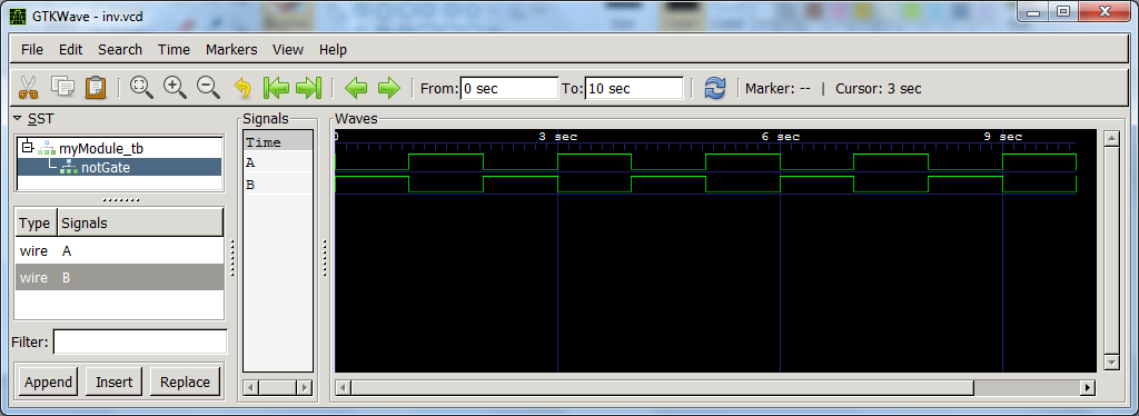
myInv simulation results
More Verilog concepts
To introduce more verilog concepts, let us design a simple arbitrator. An arbitrator is a mechanism to avoid a collision (much like a mutex in software) . For example, when a device wants to access a bus along with many other devicec connected to the bus, instead of directly accessing it, the device will place a request the arbitrator for bus access and wait for the “grant” signal. The arbitrator liaisons all such requests.
Internally, an arbitrator is a simple statemachine with the below state diagram
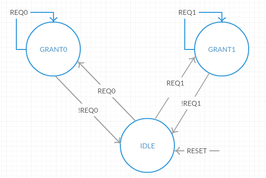
arbitrator state diagram
At a block level, an arbitrator looks like the below figure:
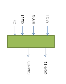
arbitrator block diagram
This article is a work in progress. I will be updating it soon with more infomration as soon as I get some time off my dayjob. :smile:


Leave a comment