

An AI-Assisted Chip Design Journey: Taping Out a VGA Demo on Real Silicon
Foreword
Every once in a while I get the itch to do something from scratch. Not a subsystem, not a block, not a firmware module dropped into somebody else’s codebase, but a full cycle, soup to nuts. Day-to-day I work very close to advanced AI accelerator silicon: RTL, emulation, low-level firmware, high-level software and python-based test infrastructure. All of it sitting inside large multi-team programmes. The work is deep and interesting, but it also means you spend a lot of time ten layers deep in somebody else’s memory controller or NoC interconnect. At some point we all start feeling FOMO and want to get back to the basics.
The final result: a VGA demo rendered gate-by-gate on a real monitor, with no CPU and no ROM.
Before Tiny Tapeout existed, scratching that itch as a hobbyist was practically impossible. EDA tool licences alone cost more than a used car, and the foundry shuttle slots that might allow a small custom tapeout were either tied to large universities or came with five-figure minimum commitments. The open-source silicon world has changed that picture completely over the last few years. Tools like Yosys, nextpnr, OpenLane/LibreLane, the Skywater 130nm and IHP 130nm open-source PDKs have come along to a point that the entire path from a .v file to a hardened GDSII runs on a laptop and in GitHub Actions, with no proprietary license in sight. Programmes like TinyTapeout, which pool many small user designs onto a single MPW shuttle wafer and handle the logistics, mean that an individual engineer like you and I can now go from RTL to physical silicon for roughly the cost of a nice dinner (OK, maybe a really nice dinner, but you get the idea).
This post is my notes from doing exactly that. The project is a VGA bouncing-text demo - “EMBEDDEDINN” drifting across a parallax starfield, rendered entirely in combinational logic with no ROM and no CPU - submitted to the TinyTapeout IHP-26a shuttle (IHP 130nm sg13g2 PDK). The two repositories live at vppillai/tinytapeout_vga (the development repo) and vppillai/tinytapeout-ihp-26a (the shuttle fork). It is a small design by gate count. It is not a small project by surface area: it touches RTL, verification, an FPGA target, a custom PCB, a logic analyzer in a closed loop, two CI pipelines, and the open-source ASIC flow. The chip is in production as I write this.
There is a second thread running through this post: almost all of the implementation grunt work was done by AI coding agents, with me as the architect - defining the design, writing the specs, reviewing everything the agent produced, and fixing the places where it went wrong. “AI wrote a chip” would be a lie. Closer to the truth: I architected a chip and ran an army of very fast, occasionally brilliant, frequently wrong junior engineers.
Why VGA
VGA is a canonical FPGA learning project for a reason. The timing requirements are rigid and well-documented, the output is immediately visible to a human, and the design is complex enough to be meaningful but small enough to be comprehensible. As a second-year RTL student you build a VGA controller almost by reflex - it sits somewhere between “blink an LED” and “implement a UART” in the standard curriculum.
In my view, VGA earns that spot for a few reasons:
- The timing is a fixed, public standard. 640x480 @ 60 Hz is just a pair of counters and some comparators. There is a right answer, and a monitor will tell you immediately and brutally whether you got it right. You don’t need advanced tools to check that you’re compliant with the spec; a simple logic analyzer shows you the timing relationships between the signals.
- It produces something you can see. A scope trace is satisfying in the lab. A picture on a monitor that you generated gate-by-gate is deeply satisfying.
- It scales in difficulty smoothly. A solid color is trivial. Bouncing animated text with a parallax background and runtime-selectable palettes is enough to exercise real design decisions about area, timing and structure - without ever needing a CPU, a bus, or external memory.
For a tapeout project those properties are genuinely useful. Because I know the domain well, I can tell immediately when the AI-generated code is wrong. Because VGA output is visual, I can validate the design at multiple stages with simulation, FPGA, and eventually silicon without needing elaborate test equipment. And because the spec is open and stable, the whole toolchain around it is mature.
There was also a slightly more specific motivation: I wanted to see whether a general-purpose language model, given careful prompting and architectural guidance, could produce synthesisable RTL that was also tapeout-quality. That is a meaningfully harder bar than “synthesises without errors.” Synthesisable RTL for an FPGA is permissive as timing is handled by the PnR tools and you have room to iterate in minutes. RTL for a tapeout has to be correct the first time. There is no patch iteration once the GDS tape goes to the fab.
How VGA actually works (the 60-second crash course)
VGA is a raster scan protocol. A pixel clock drives two counters : one horizontal (hpos) and one vertical (vpos) , that together describe where the electron beam is at any given moment. When hpos is within the active display region (0-639 for 640×480) and vpos is within the active region (0-479), the R, G, and B signals carry the colour of that pixel. Outside those regions, the colour signals must be zero (black), and the sync pulses encode the start of a new line (hsync) and new frame (vsync).
At 640x480 @ 60 Hz the numbers are:
| Parameter | Horizontal | Vertical |
|---|---|---|
| Display | 640 | 480 |
| Front porch | 16 | 10 |
| Sync pulse | 96 | 2 |
| Back porch | 48 | 33 |
| Total | 800 | 525 |
800 x 525 x 60 Hz = 25.2 MHz, which is why the canonical VGA pixel clock is 25.175 MHz. Get that clock wrong and the monitor either refuses to lock or rolls the image.
The failure mode most beginners hit is outputting non-zero colour values outside the active display area. Some monitors tolerate this, some don’t, and it causes subtle artefacts or no-sync conditions on others. The correct pattern is:
assign rgb = (display_on) ? active_rgb : 6'b000000;
where display_on is the combinational AND of hpos < H_DISPLAY and vpos < V_DISPLAY. The hvsync_generator module in this project handles this cleanly.
Another subtlety: sync polarity matters. For 640×480@60Hz both hsync and vsync are active low. Getting this wrong results in a “connected but no signal” condition on many modern monitors, even if the pixel data is correct. And if you sample asynchronous inputs (a reset button, a vsync edge used for animation) without care, you get jitter that shows up as a twitchy image.
Every one of these is a thing I knew to watch for, and every one of them is a thing I had to make sure the agent did not get wrong. Domain knowledge and design expertise is not optional when using AI agents for design code generation. You have to know the spec and the common failure modes cold, because you are going to be debugging those exact issues in simulation, on FPGA, and eventually on silicon.
The TinyTapeout VGA pin mapping
TinyTapeout exposes 8 output bits (uo_out[7:0]). The standard TinyVGA PMOD from mole99 expects a specific packing of those 8 bits into a 2-bit-per-channel RGB222 signal plus sync:
uo_out[7] = HSYNC    uo_out[3] = VSYNC
uo_out[6] = B[0]     uo_out[2] = B[1]
uo_out[5] = G[0]     uo_out[1] = G[1]
uo_out[4] = R[0]     uo_out[0] = R[1]
This is a well-established convention in the TinyTapeout community - understanding it upfront and baking it into the module interface saves a lot of pain later.
The operating model: architect up front, agents on the keys
I approached this exactly the way I approach a large program at work, just compressed and with a very fast team. The phases that I consider “the real work” - the parts I enjoy and would never delegate - I did myself:
- I decided the design must be a single-tile VGA demo with a no-ROM generative font, a parallax starfield, and runtime controls. The “no ROM” decision is an architectural one: it trades a small amount of combinational logic for zero memory, which is exactly the right call on a one-tile budget.
- I defined the verification strategy: a
cocotbsuite that checks timing against the VGA spec, plus aVerilatorpipeline that renders the actual output to a GIF so I could see regressions, not just read pass/fail. - I planned the hardware bring-up as a sequence of increasingly ambitious experiments - clock first, then a square wave on a pin, then the full design - with a logic analyzer in the loop so the agent had ground truth instead of my opinion.
- I owned the CI/CD topology, the repo split, the token scoping, and the submission flow.
The agents did the typing. And here is the caveat : RTL is the hardest domain I have used coding agents in, and it is not close. The general-purpose models a hobbyist can reach are trained on an internet that is saturated with Python and JavaScript and starved of good, synthesizable, well-verified Verilog. So the models are confidently mediocre at hardware. They will write code that simulates and does not synthesize, or synthesizes and does not meet timing, or meets timing and quietly infers a latch. Every interesting line in this project survived because I knew what correct looked like and could verify it. You have to keep pushing until the agent gets there. The leverage is enormous, but it amplifies the designer’s judgment rather than replacing it.
Where the agents earned their keep was volume and plumbing. The 850-line cocotb suite, the Verilator harness, the Makefiles, the two CI pipelines - that is a lot of careful, tedious, easy-to-get-subtly-wrong code, and they produced it far faster than I would have. They also closed the toolchain loop mostly on their own: downloading and configuring oss-cad-suite, wiring up apio, and iterating on pin constraints against logic-analyzer captures, largely autonomously once I had defined the experiment. And a couple of times they genuinely out-thought my first draft - the starfield’s XOR formulation and the browser-frame-rate compensation in the GIF exporter are two ideas I’ll call out in the walkthrough where the agent landed somewhere cleaner than my first instinct.
At the end of the day it is practically my code. The agents typed it, and occasionally they improved on my sketch. Typing and orchestration I delegated; architecture and judgment I kept - that is the whole thesis of this post.
The RTL, and the parts worth bragging about (a little)
The whole design is one Verilog file, vga_tt.v, with two modules: a sync generator and the renderer. Here is the top-level structure.
                    ┌──────────────────────────────────────────────────────┐
                    │              tt_um_embeddedinn_vga                   │
  clk (25MHz) ──────┤──┬───────────────────────────────────────────────────│
  rst_n ────────────┤──┼─────┐                                             │
  ui_in[7:0] ───────┤──┼─────┼──────────────────┐                          │
                    │  ▼     ▼                  │                          │
                    │ ┌─────────────────┐    ┌──┼───────────────────┐      │
                    │ │ hvsync_generator│    │  │ Text & Starfield  │      │
                    │ │   hpos[9:0] ────┼───►│  │    Renderer       │      │
                    │ │   vpos[9:0] ────┼───►│  │ procedural font   │      │
                    │ │   hsync/vsync ──┼────┼──┼──────────────┐    │      │
                    │ │   display_on ───┼───►│  ▼              │    │      │
                    │ └─────────────────┘    │ [1:0] Speed     │    │      │
                    │                        │ [3:2] Palette   │    │      │
                    │                        │ [4]   Scanline  │    │      │
                    │                        └───────┬─────────┘    │      │
                    │                                ▼              ▼      │
                    │                        ┌─────────────────────────┐   │
                    │                        │    Output Packing       │   │
                    │                        │ {hsync,B0,G0,R0,        │   │
                    │                        │  vsync,B1,G1,R1}        │   │
                    │                        └────────────┬────────────┘   │
                    └─────────────────────────────────────┼────────────────┘
                                                           ▼
                                                     uo_out[7:0]
The sync generator (the boring, load-bearing part)
There is nothing novel here. The hvsync_generator is the standard two-counter VGA timing block that you will find in essentially every Tiny Tapeout VGA example. It counts pixels and lines and derives the sync and display_on strobes:
module hvsync_generator(
    input wire clk,
    input wire reset,
    output reg hsync, vsync, display_on,
    output reg [9:0] hpos, vpos
);
  localparam [9:0] H_DISPLAY = 640, H_FRONT = 16, H_SYNC = 96;
  localparam [9:0] V_DISPLAY = 480, V_FRONT = 10, V_SYNC = 2;

  always @(posedge clk or posedge reset) begin
    if (reset) begin
      hpos <= 0; vpos <= 0; hsync <= 0; vsync <= 0; display_on <= 0;
    end else begin
      if (hpos < 799) hpos <= hpos + 1;
      else begin
        hpos <= 0;
        if (vpos < 524) vpos <= vpos + 1; else vpos <= 0;
      end
      hsync <= !((hpos >= H_DISPLAY + H_FRONT) && (hpos < H_DISPLAY + H_FRONT + H_SYNC));
      vsync <= !((vpos >= V_DISPLAY + V_FRONT) && (vpos < V_DISPLAY + V_FRONT + V_SYNC));
      display_on <= (hpos < H_DISPLAY) && (vpos < V_DISPLAY);
    end
  end
endmodule
The generative font engine (this is the fun part)
The thing I am actually proud of is the font - though it is not entirely my brainchild. It draws on other implementations, and the agent helped me spot a few patterns. On a single Tiny Tapeout tile there is no room for a character ROM, so the letters are built out of logic. Each character gets a 32-pixel-wide slot; the renderer derives a within-character coordinate and then constructs glyphs from a tiny vocabulary of bars:
// Position of the current pixel relative to the moving text box
wire [9:0] rx = pix_x - {1'b0, tx};
wire [9:0] ry = pix_y - {1'b0, ty};

wire [3:0] char_idx = rx[8:5];   // which character (32px slots)
wire [4:0] lx        = rx[4:0];  // x within the character (0..31)
wire [3:0] ly        = ry[5:2];  // y within the character (rows of 4px)

// Shape primitives - construct letters from bars to save gate space
wire left_bar  = (lx < 4);
wire right_bar = (lx >= 16 && lx < 20);
wire top_bar   = (ly == 0);
wire mid_bar   = (ly == 5);
wire bot_bar   = (ly == 9);
wire corner    = (top_bar || bot_bar || mid_bar) && right_bar;
With that vocabulary, a letter is just a boolean expression. EMBEDDEDINN happens to need only the glyphs E, M, B, D, I and N, and the char_idx selects which boolean to evaluate for the current pixel:
case (char_idx)
  4'd0, 4'd3, 4'd6: pix = left_bar || top_bar || mid_bar || bot_bar;                       // E
  4'd1:             pix = left_bar || right_bar || (lx >= 8 && lx < 12 && ly < 6);          // M
  4'd2:             pix = (left_bar || right_bar || top_bar || mid_bar || bot_bar) && !corner; // B
  4'd4, 4'd5, 4'd7: pix = left_bar || ((top_bar || bot_bar) && lx < 16) || (right_bar && !top_bar && !bot_bar); // D
  4'd8:             pix = (lx >= 8 && lx < 12);                                             // I
  4'd9, 4'd10:      pix = left_bar || right_bar || (ly == lx[4:2] + 2);                     // N
  default:          pix = 0;
endcase
There is a real trick hiding in here. The eleven characters of EMBEDDEDINN collapse to six unique expressions because the repeats (E at indices 0/3/6, D at 4/5/7, N at 9/10) share logic. The N diagonal is my favorite line - ly == lx[4:2] + 2 draws a slash by tying the vertical position to a shifted horizontal position, so the stroke falls naturally across the glyph with almost no gates. This is the kind of code where I’d sketch the idea (“bars plus a couple of diagonals, no ROM, share glyphs”), the agent would produce a first cut, and we’d iterate pixel by pixel against the rendered GIF until each letter was legible. The concept is mine; a fair amount of the bit-fiddling convergence was the agent grinding against my acceptance criterion of “it has to be readable on a real monitor.”
NOTE: The font is also where you feel the area budget - every additional primitive is gates. I deliberately kept the vocabulary tiny and let the glyphs look a little brutalist: on one tile, elegance is measured in cells, not curves. ;)
The parallax starfield (an agent idea I kept)
The background is a two-layer starfield, and the formulation is one of the places an agent proposed something I liked better than my first sketch. A “star” is simply a pixel where an XOR of the screen coordinate against the frame counter lands on a diagonal:
wire star_f = ((pix_x[5:0] ^ frame_cnt[5:0])  == (pix_y[5:0] ^ frame_cnt[11:6]));
wire star_s = ((pix_x[5:0] ^ frame_cnt[7:2])  == (pix_y[5:0] ^ frame_cnt[13:8]));
Two layers, tapped from different bits of the same free-running frame_cnt, scroll at different apparent speeds and give you parallax for almost nothing. There is no star storage anywhere - the field is purely a function of position and time. I had been thinking about a more complex LFSR; the XOR-diagonal version is cheaper and looks better, and I am happy to give credit where it is due.
Color, controls, and packing for the PMOD
The renderer mixes a palette (selectable at runtime), a subtle text color-cycle, and an optional scanline effect, all driven off ui_in. The interactive bits are deliberately cheap - a couple of comparators on the dedicated input pins:
// Speed control via ui_in[1:0]: normal / fast(2x) / slow / pause
wire [1:0] speed_sel = ui_in[1:0];
wire move_en = (speed_sel == 2'b11) ? 1'b0          : // Pause
               (speed_sel == 2'b10) ? frame_cnt[0]  : // Slow (every other frame)
                                      1'b1;            // Normal / Fast
wire [1:0] step = (speed_sel == 2'b01) ? 2'd2 : 2'd1; // Fast = double step
Animation is advanced on the rising edge of vsync, detected synchronously so there is no cross-domain jitter :
wire vsync_rising = vsync && !vsync_prev;
// ... inside always @(posedge clk):
vsync_prev <= vsync;
if (vsync_rising) begin
    frame_cnt <= frame_cnt + {14'b0, step};
    if (move_en) begin
        tx <= x_dir ? tx - {7'b0, step} : tx + {7'b0, step};
        ty <= y_dir ? ty - {7'b0, step} : ty + {7'b0, step};
        if (tx >= 280) x_dir <= 1; else if (tx <= 10) x_dir <= 0;
        if (ty >= 420) y_dir <= 1; else if (ty <= 10) y_dir <= 0;
    end
end
Finally, the eight output bits are packed into the layout the TinyVGA PMOD by mole99 expects - a resistor-DAC giving two bits per channel:
assign uo_out = {hsync, b[0], g[0], r[0], vsync, b[1], g[1], r[1]};
That packing line is innocent-looking and cost me real time on hardware. More on that in the bring-up section.
Verification: simulate, then see
Two things check this design. The first is a cocotb suite; the second is a Verilator renderer that turns the RTL into a GIF.
22 cocotb tests, grouped for wall-clock
The suite (test/test.py) is 22 tests across four categories - timing, video output, animation/features, and design verification. The timing tests are the load-bearing ones, because they assert the VGA spec directly. For example, HSYNC width is checked to be exactly 96 clocks within a one-clock tolerance:
@cocotb.test()
async def test_hsync_pulse_width(dut):
    # ... reset, start 25 MHz clock ...
    await wait_hsync_fall(dut)
    count = 0
    while get_hsync(dut) == 0:
        await RisingEdge(dut.clk)
        count += 1
    assert H_SYNC - HSYNC_TOL <= count <= H_SYNC + HSYNC_TOL
There are tests for sync polarity, sync period (800 clocks/line, 420000 clocks/frame), black-during-blanking, valid 2-bit color range, the exact uo_out packing order, the text appearing at its known reset position, “pause” actually freezing the glyph, and the starfield producing varied pixels. The full list lives in test/README.md.
The parallel test harness is another place the agent did something tidy. The tests are bucketed into five groups balanced by estimated wall time, each running in its own simulator build directory so they don’t stomp on each other:
_g_anim:
 $(MAKE) TESTCASE=test_animation \
  SIM_BUILD=sim_build/g_anim COCOTB_RESULTS_FILE=results_anim.xml
# ...four more groups...
test-parallel: _g_anim _g_speed _g_visual _g_frame _g_fast
 @echo "All parallel test groups passed"
make -j5 test-parallel then runs them concurrently for roughly a 2x speedup locally and in CI. It is a small thing, but it is exactly the kind of “engineer the test loop early” hygiene I’d insist on at scale.
The GIF pipeline: making the RTL watchable
A green test suite tells you the timing is right; it says nothing about whether the picture looks right. I wanted to see the output and catch the regressions a human notices instantly - a letter that lost a stroke, or a palette gone muddy, the kind of thing that is nearly impossible to spot in a waveform. So the design renders itself to an animated GIF, and that GIF is what you see at the top of the repo README.
The flow is: Verilator compiles vga_tt.v into a fast native model; a small C++ driver (test/vga_sim.cpp) clocks it, walks the raster exactly like a monitor would, and dumps raw RGB frames; then test/make_gif.py assembles them. The C++ driver follows the sync signals to find the active region:
// Wait for vsync, skip the back porch, then capture 480 active lines
for (int y = 0; y < V_DISPLAY; y++) {
    // align to active pixels after H_BACK...
    for (int x = 0; x < H_DISPLAY; x++) {
        uint8_t val = dut->uo_out;        // {hsync,b0,g0,r0,vsync,b1,g1,r1}
        uint8_t r = ((val >> 0) & 1) << 1 | ((val >> 4) & 1);
        uint8_t g = ((val >> 1) & 1) << 1 | ((val >> 5) & 1);
        uint8_t b = ((val >> 2) & 1) << 1 | ((val >> 6) & 1);
        frame_data.push_back(COLOR_MAP[r]); // 2-bit -> {0,85,170,255}
        // ...
    }
}
It captures 540 frames - one full horizontal bounce cycle, about nine seconds at 60 Hz - so the GIF loops cleanly.
Then there’s a subtlety I would not have bothered with, and the agent flagged: GIFs lie about time in browsers. The GIF format specifies frame delays in centiseconds, and most browsers enforce a ~20 ms floor, so a true-60 Hz (16.67 ms) capture plays back slow on a web page. The fix is to export two GIFs - a frame-accurate one, and a “browser-compensated” one that drops every sixth frame so it plays at the right real-time speed despite the 20 ms floor:
# Browser enforces ~20ms/frame (50 fps). To keep real-time speed at 60 fps
# source, keep ~5/6 of frames so playback duration matches reality.
preview_indices = [int(i * 1.2) for i in range(len(frames) * 5 // 6)]
preview_frames  = [frames[i] for i in preview_indices if i < len(frames)]
save_gif(preview_frames, Path("vga_preview.gif"), 20, "browser-compensated")
That is a genuinely nice catch. The hardware runs at true 60 Hz regardless; this only matters for the README animation. The whole GIF job runs in CI after tests pass and auto-commits the result.
The Verilator-rendered preview, which was the agent's main feedback mechanism during design and verification.
Hardware in the loop: FPGA, a custom board, and a logic analyzer in a closed loop
Simulation is an opinion until silicon (or at least an FPGA) agrees with it. Long before the ASIC flow, I brought the design up on a Lattice iCEstick (iCE40HX1K), because validating on a real device de-risks everything downstream. I used the apio toolchain, which wraps Yosys and nextpnr for iCE40 targets. This also makes it easy for the agent to drive the whole flow end to end - from Verilog to bitstream to flash.
Clock first, always
The iCEstick has a 12 MHz crystal; VGA wants 25.175 MHz. So the first thing on the board is a PLL, and the first thing I validate is only the PLL. The shared pll_25mhz.v wraps the iCE40 hard PLL:
SB_PLL40_CORE #(
    .FEEDBACK_PATH("SIMPLE"),
    .DIVR(4'b0000),     // /1
    .DIVF(7'b1000010),  // x67
    .DIVQ(3'b101),      // /32
    .FILTER_RANGE(3'b001)
) pll_inst ( .REFERENCECLK(clk_in), .PLLOUTCORE(clk_out), .LOCK(locked), ... );
12 MHz x 67 / 32 = 25.125 MHz. That is ~0.2 % under the ideal 25.175, which the monitor I tried on tolerates without complaint. It was a good reminder that VGA is forgiving on pixel clock but not on sync. I bring the PLL up on its own with a tiny “walking LED” test whose only job is to prove the locked signal asserts and the 25 MHz domain is alive before any VGA logic is in the picture. Bring-up discipline: prove the clock, then build on it.
A VGA adapter board, lightly modified
The iCEstick doesn’t have a VGA connector, so the RGB-plus-sync pins go out through a TinyVGA-style PMOD: a small resistor-DAC board that turns two bits per channel into analog VGA levels. I took the open-source mole99 tiny-vga design, made minor modifications to optimise for JLCPCB assembly, and had it fabbed at JLCPCB. A few images from the process are below.
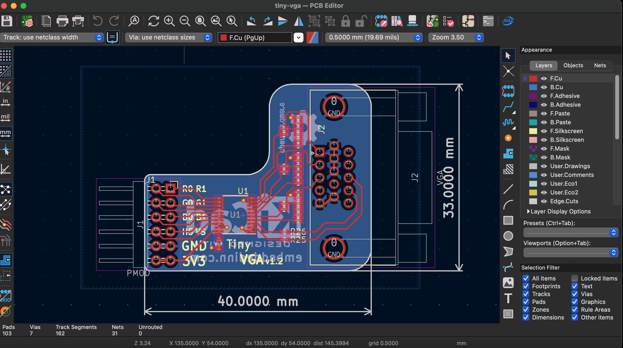
the board after modifications in Kicad layout view
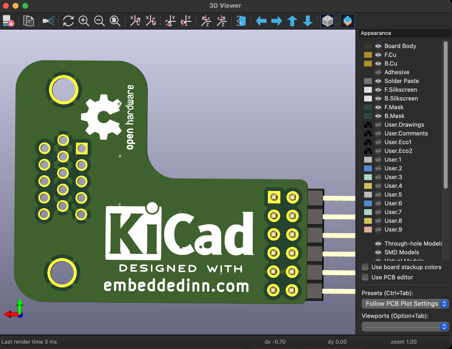
the board after modifications in 3D view
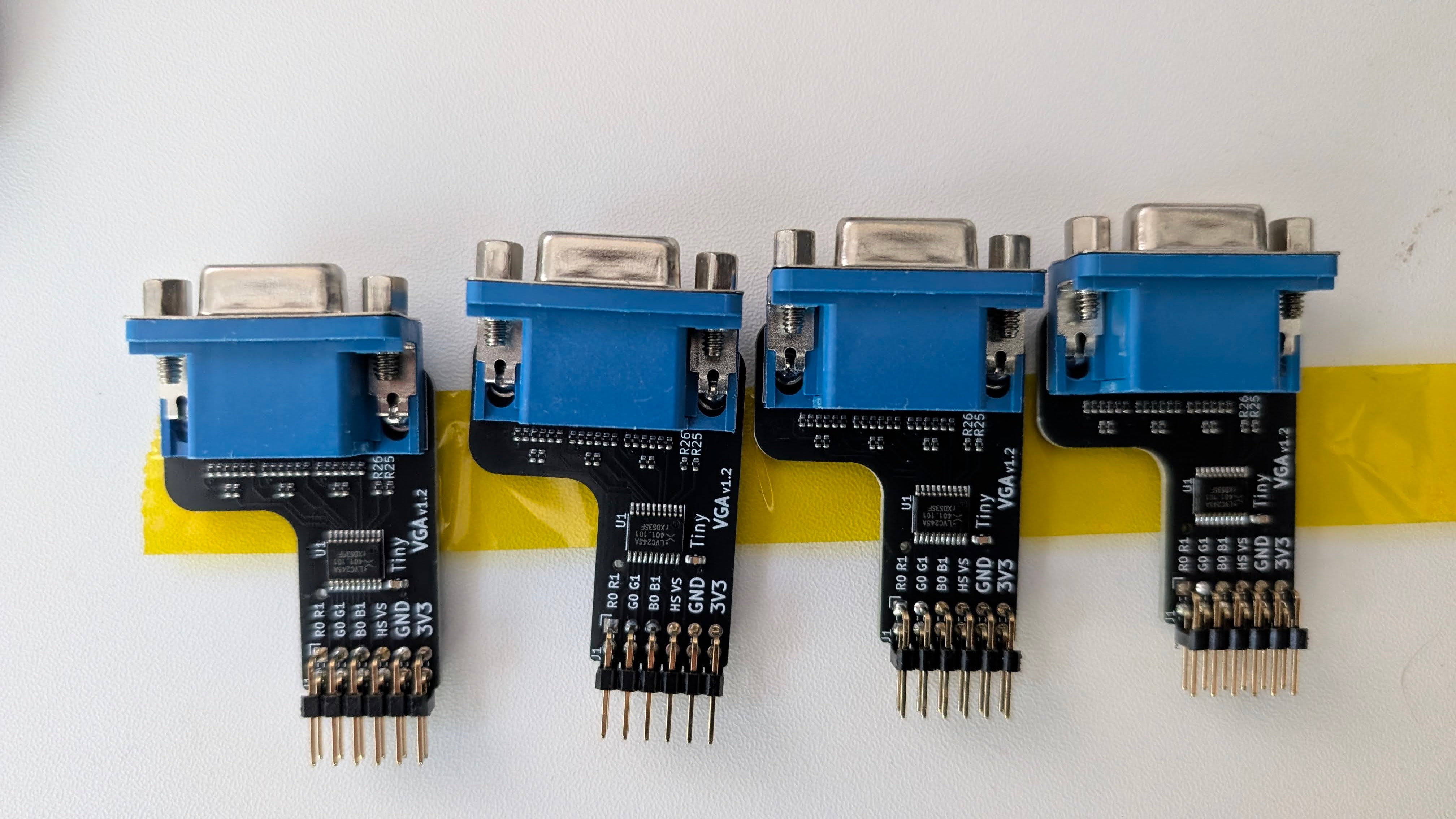
The custom PMOD adapter board, based on mole99's TinyVGA design as sent from JLCPCB
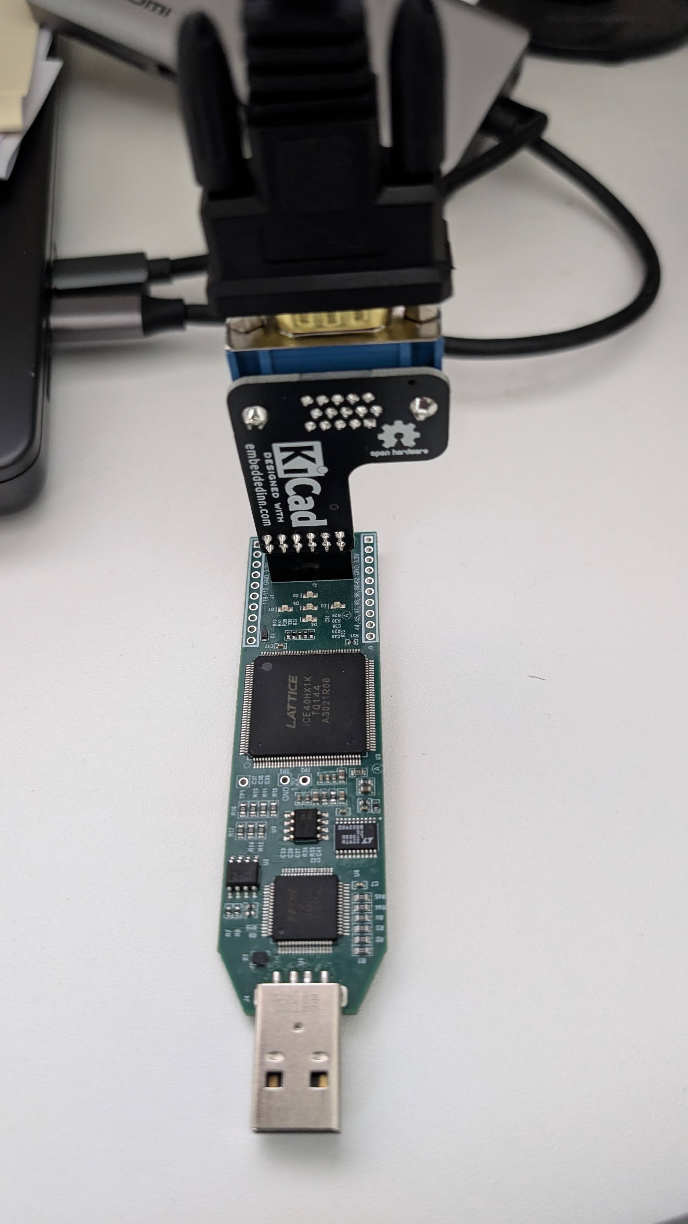
The iCEstick + VGAmod adapter in its early bring-up phase
Closing the loop with a logic analyzer
Here is the part I think is most interesting methodologically. Rather than eyeball a monitor and guess, I put a Saleae logic analyzer on the output pins and fed its captures back to the agent as ground truth, so the toolchain bring-up ran as a closed loop: the agent would build a bitstream with apio (driving Yosys for synthesis and nextpnr for place-and-route under the hood), flash it, trigger a capture through Saleae’s Python automation, and compare the measured pin behavior against the expected timing - then fix and repeat.
   ┌─────────────┐   build/flash    ┌────────────┐    drives    ┌──────────────┐
   │  AI agent   │ ───────────────► │  iCEstick  │ ───────────► │  Saleae LA   │
   │ (apio/yosys │                  │  (FPGA)    │              │  capture     │
   │  /nextpnr)  │ ◄─────────────── │            │ ◄─────────── │  (Python)    │
   └─────────────┘   waveforms /    └────────────┘   pin probe  └──────────────┘
                     pass-fail
The very first automated experiment was deliberately trivial: generate a square wave and confirm it on a pin. That isolates “can the agent drive the whole flow end to end - download and install oss-cad-suite, synthesize, route, build a bitstream, flash it, and read back reality” from “is the VGA design correct.” Once the square wave was solid, scaling up to the real design was mostly a matter of pin constraints. We iterated a fair bit there - the iCEstick-to-PMOD pin map in the .pcf took a couple of passes - but the agent converged on a working flow almost autonomously once the experiment and the success criterion were defined.
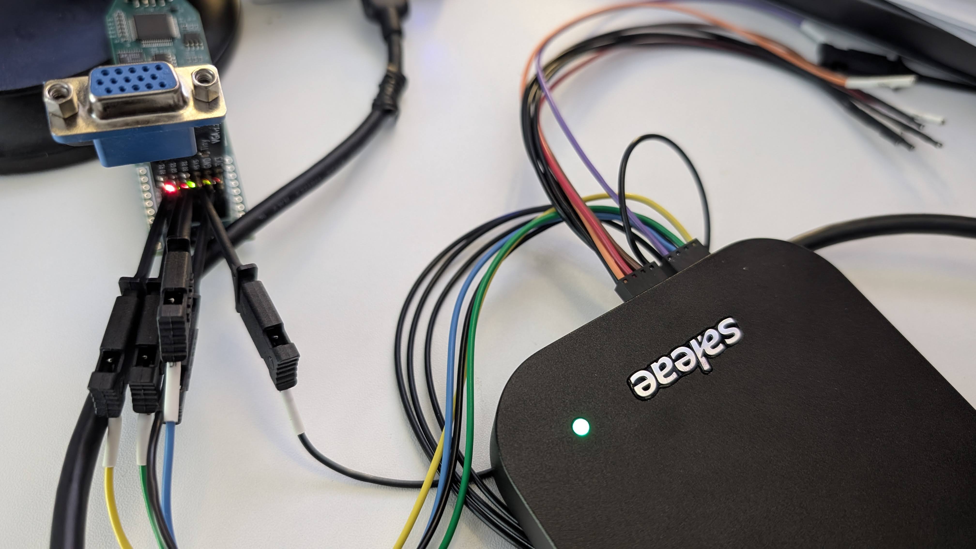
The fpga board and adapter hooked up to the Saleae logic analyzer for closed-loop bring-up. The agent drove the whole flow - from Verilog to bitstream to flash to capture - with the Saleae captures as ground truth for debugging.
A couple of real bugs from that phase, straight out of the commit log, because they’re the honest texture of hardware bring-up. The first was a floating reset pin: the design depended on a reset input that wasn’t actually driven on the board, so the fix was to stop depending on it and let the design auto-start once the PLL locks. Classic - works in sim, floats on the bench. The second was color bit-ordering, which got swapped between the uo_out packing and the capture/decoder more than once. That single packing line I flagged earlier is exactly the kind of thing that is trivially right in your head and trivially wrong in the wiring.
For the final aesthetic tuning - palette choices, the scanline look, the bounce bounds - I also leaned on the Tiny Tapeout VGA Playground to fiddle with the output interactively before baking choices back into the RTL.
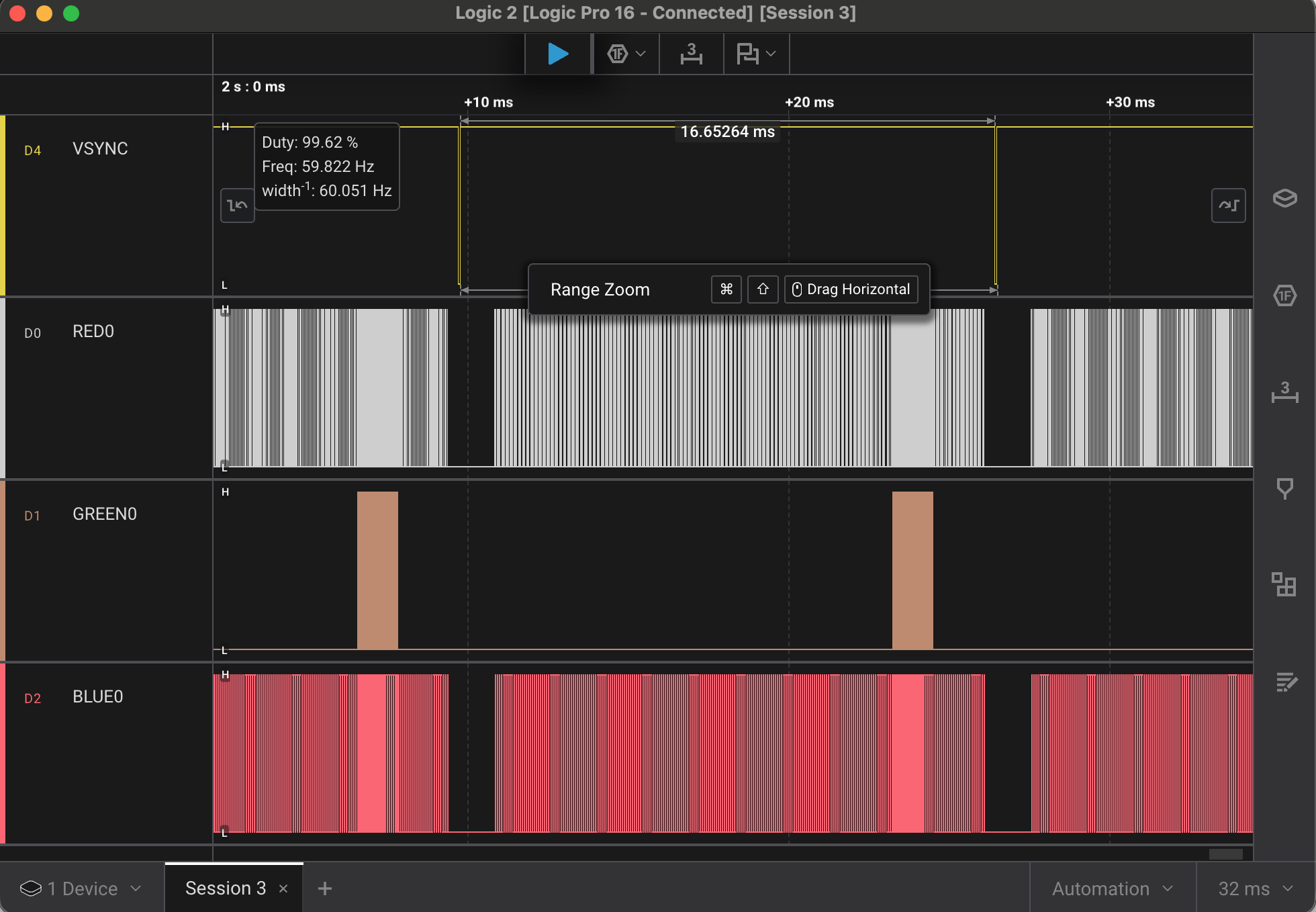
A Saleae capture showing the output waveforms.
CI/CD: two pipelines and a sync architecture
I treat infrastructure as a first-class part of any project, hobby or not, and this one has more of it than the RTL. There are effectively two layers of CI.
The short version: the code is split across two repos - the development repo (tinytapeout_vga) where the design and tests live, and the submission repo (tinytapeout-ihp-26a) which is a fork of the IHP shuttle template and contains only the files relevant to the shuttle submission. The development repo has a comprehensive CI pipeline that runs on every push and checks everything - it is the “workshop” where I iterate fast with confidence. The submission repo has a more gate-gated pipeline that runs the full Tiny Tapeout precheck, GDS generation, verification, and datasheet checks - it is the “assembly line” that ensures nothing gets to the shuttle without passing all the gates. When a change is made in the development repo, a sync job copies the relevant files to the submission repo immediately, without waiting for tests, because the submission pipeline is the gate that matters for correctness.
My pipeline
My own ci.yml runs on every push: it installs uv and the apio packages, runs the parallel cocotb suite, builds the FPGA bitstream as an artifact, and - after tests and build pass - regenerates the preview GIF and commits it back with a [skip ci] tag so it doesn’t loop. The design also keeps a single source of truth for shared components: the PLL lives in one place and is synced into both the VGA build and the LED test before each build, so a PLL change can’t silently diverge.
The dual-sync to Tiny Tapeout
The more interesting piece is how my development repo feeds Tiny Tapeout. I keep a clean separation: my repo is the workshop (FPGA wrapper, board files, LED test, GIF tooling), and only the submission-relevant files are mirrored out. A GitHub Actions job watches for changes to the files that actually matter and syncs them to two places - the full IHP shuttle repo and a clean submission template - immediately, without waiting for tests:
sync-tt:
  needs: []   # sync immediately; the submission repo runs the comprehensive checks
  if: (github.event_name == 'push' && github.ref == 'refs/heads/main') || ...
  steps:
    - name: Check for TT-relevant changes
      run: |
        if git diff --name-only HEAD~1 HEAD | grep -qE \
          '^(src/(vga_tt\.v|info\.yaml|config\.json)|docs/(info\.md|README\.md)|test/...)$'; then
          echo "tt_changed=true" >> $GITHUB_OUTPUT
        fi
    - name: Sync files to TT repo   # copies vga_tt.v, info.yaml, tests into projects/tt_um_embeddedinn_vga/
tinytapeout_vga
(workshop)"] subgraph CI["GitHub Actions"] T["cocotb tests
(parallel)"] B["FPGA bitstream"] G["preview GIF
(auto-commit)"] S["change-gated sync"] end SH["IHP shuttle repo
tinytapeout-ihp-26a"] SUB["submission template
tt-vga-submission"] TT["Tiny Tapeout flow
precheck · gds · verify · datasheet"] DEV --> T --> B --> G DEV --> S S --> SH S --> SUB SH --> TT SUB --> TT
The design choice worth naming: sync is decoupled from local tests on purpose. Local tests exist for fast FPGA iteration; the authoritative checks are the comprehensive ones that run in the submission repo (precheck, gds, verification, tt_datasheet). So I optimize my inner loop for speed and let the shuttle’s pipeline be the gate that matters.
Letting an agent touch GitHub, safely
To automate the development loop, I gave an agent scoped, limited-access tokens so it could operate GitHub on its own, and the guardrails were the point. The tokens were narrowly scoped - just enough to do the job, revocable, and never my personal credentials. Beyond the very first commit, the agent had to open pull requests rather than push to main, so every change stayed reviewable. And the whole flow stayed observable end to end: agent scratch directories are git-ignored, CI is the choke point, and nothing reaches the shuttle without passing through the change-gated sync.
This is exactly how I’d onboard a fast junior to a repo I cared about: scope the access, make them propose changes, and put the real gates in CI.
The ASIC flow and the submission
The submission target is the Tiny Tapeout IHP 26a shuttle - the IHP SG13G2 130 nm open-source process, the EU-fabricated successor to the SkyWater-based shuttles. Hardening uses LibreLane (the OpenROAD-based flow), driven by a config.json that I kept close to the Tiny Tapeout defaults, tuning only what the design needed:
"CLOCK_PERIOD": 20,           // 20ns == 50MHz timing target (comfortable for 25MHz pixel clock)
"PL_TARGET_DENSITY_PCT": 60,  // single-tile, no congestion pressure
"RUN_LINTER": 1,              // keep the linter on - it caught real issues
That linter line matters. I left it on, and it forced me to handle every unused signal explicitly (there’s a deliberate _unused sink in the RTL for exactly that) and to chase down an unclocked-register warning during bring-up. Turning the linter off would have been the easy, wrong choice.
The Tiny Tapeout pipeline then does the heavy physical lifting in the shuttle repo: precheck, gds (synthesis through place-and-route to a hardened GDSII, with the gate-level netlist used for gate-level simulation), verification, and tt_datasheet. The artifacts those jobs publish - the 2D GDS render, the 3D die view, the placement images, the datasheet - are how you confirm your tile actually closed.
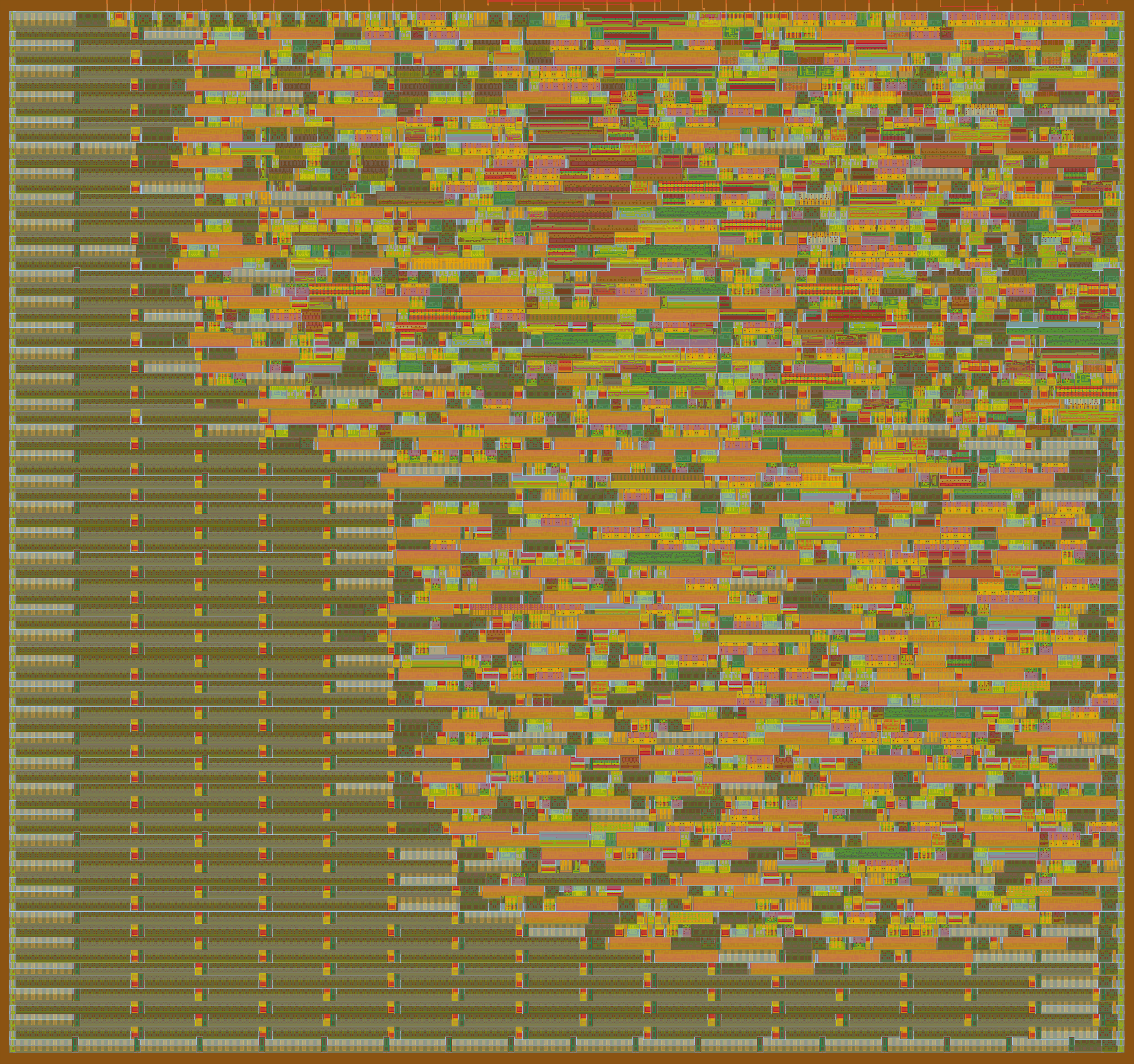
The 2D GDS render of the hardened design
The LibreLane place-and-route run for this design placed the logic at reasonable density within the single-tile area allocated by TinyTapeout. The 3D render from the GDS workflow shows the standard cells laid out in rows with the metal routing above them. It is a small design - the entire thing fits in the TinyTapeout tile with some room to spare - but seeing it laid out in silicon layers is still satisfying.
The font logic accounts for a disproportionate share of the cell count: eleven characters × 7 rows × 8 columns = 616 pixel decisions, each requiring a small combinational expression. The synthesis tool does a reasonable job of sharing logic between identical letters (the two ‘E’s, the two ‘D’s, etc.) but it still shows up in the area report.
The 3D GDS render of the hardened design, which is also published as an interactive WebGL view in the datasheet
You can see this interactive 3D view at the interactive GDS viewer.
The published shuttle page for this tile is at the Tiny Tapeout shuttle page.
How to actually submit
The submission mechanics took me longer to figure out than they should have, so here’s the condensed checklist:
- Start from the right template. Fork/clone the official IHP Verilog template (
TinyTapeout/ttihp-verilog-template) - not a SkyWater one. Submitting a SkyWater-hardened design to an IHP shuttle fails the precheck with a PDK-mismatch error. - Drop in your files.
src/<your_top>.v,info.yaml(top module must start withtt_um_, settiles,clock_hz, and the full pinout),docs/info.md, andtest/(Makefile,tb.v,test.py, README). I automate this copy with amake tt-release/ sync job so the submission repo is always a clean mirror. - Fill in
info.yamlhonestly. Title, author, language, clock, tile count, and - importantly - the pin descriptions, because they show up in the datasheet. - Enable GitHub Pages → Source: GitHub Actions on the submission repo so the datasheet/render pages build.
- Let the workflows run and go green.
precheckfirst (it catches the silly stuff), thengds,verification,tt_datasheet. Red precheck = fix before anything else. - Inspect the published artifacts. Look at the GDS/3D render and the gate-level results to confirm your design hardened the way you expect - not just that the job passed.
- Submit the repo through the Tiny Tapeout submission flow and keep iterating up to the shuttle deadline; you can keep pushing fixes until it closes.
What the whole loop taught me
Two things stuck with me.
The first is that AI multiplies judgment; it doesn’t stand in for it. Having an army of capable agents to tap into let me run this exactly like a large program: set up CI on day one, stand up the simulation framework and the visual regression early, put hardware-in-the-loop with the FPGA and the logic analyzer wired to the agents, and keep a human in the loop for the visual sign-off that no test fully captures. Those are standard practices I’d apply to anything I was building at scale, and the agents let me apply all of them to a hobby project in evenings, because the marginal cost of “do it properly” dropped through the floor. The leverage is real. But every interesting line survived because I knew what right looked like. On RTL the models are still mediocre in ways that look confident, and the project worked precisely because I treated them like talented juniors on an unfamiliar codebase - clear specs, tight feedback loops, and no change merged without review.
The second is about the craft itself. Driving one small design through the entire cycle - architecture, RTL, verification, an FPGA, a PCB, a logic analyzer, the open ASIC flow - is the best way I know to take stock of where the state of the art actually is. The open-source silicon stack has gotten good. The agent tooling has gotten genuinely useful, with sharp edges in exactly the places you’d predict from how these models were trained. Doing the loop yourself, and being honest about which parts you did and which parts the machine did, is how you keep your map of the territory current. That, more than the bouncing text, is what I got out of this.


Leave a comment