

A Desktop QSFP-DD Tester for 400G Cables and Optics, Part 2: The Cable, CMIS and the Board
Previously: Part 1 told the whole story in short: AI agents took a QSFP-DD cable tester board from my brief to a filled-in JLC order, under rules and specs I wrote, and the power, management and firmware paths on the boards work, while signal testing is still open. This part is the hardware itself: what the tester talks to, how, what is on the board and why each part sits where it does.
Tools in this part
| Tool | What it does here |
|---|---|
pyftdi |
A pure-Python driver for FTDI chips over libusb. It lets us use the FT2232H’s MPSSE engine as an I2C master and GPIO pins for the laptop. |
| LCSC and JLC part pages | Live stock, package and Basic or Extended status for every part number, fetched by a component engineer agent before it enters the BOM. |
| DigiKey’s product API | The same live check for the case hardware (light pipes, feet, magnets), with exact part-number matches only. |
1. History lesson: A host with the fast lanes left out
Part 1 introduced the active electrical cable, copper with a small DSP-powered module in each plug. Whatever sits in the QSFP-DD (Quad Small Form-factor Pluggable Double Density) cage, cable or optic, expects a host on the other side, normally a switch or a network interface card (NIC). The host gives the module a 3.3V supply (good for anything from about 1.5W in the smallest power class to well over 10W in the largest), a slow management bus made of I2C plus a handful of single-ended sideband pins, and then the fast stuff, eight lanes of serial data in each direction on sixteen differential pairs, 32 pins in all.
My tester acts as a a host with the fast stuff left out. Each unit, the AEC-CT2-MINI, is one QSFP-DD cage on a 42 × 136 mm “stick”. It gives the module a proper 3.3V rail, the I2C bus and every sideband pin, and leaves all 32 high-speed pins unconnected (untill v1 ;) ) . One unit goes on each end of the cable under test, and the test software plays host to both ends at once.
1.1 Why copper grew a DSP
At high speeds a copper wire ends up acting as a a low-pass filter with ambitions. A 400G host interface (400GAUI-8) runs eight lanes of 53.125 Gb/s, and an 800G one (800GAUI-8) runs eight lanes of 106.25 Gb/s. Both use PAM4, which has four voltage levels and carries two bits per symbol, so a 106.25 Gb/s lane only switches at 53.125 GBd and the copper sees half the bandwidth that two-level NRZ (non-return-to-zero) signalling would need. You pay for that in noise margin. Because of the 4 voltage levels, PAM4 stacks three eyes inside the same swing, so each eye is a third of the height of a single NRZ eye with the same peak-to-peak voltage, about 9.5 dB smaller (20 log10 3). Every metre of twinax adds loss that grows with frequency, and the Nyquist frequency of a 53.125 GBd lane sits at about 26.6 GHz. (Honestly, I dont have most of these numbers in my head on a daily basis. I had to look them up for writing this paragraph. But the concept is critical to understand while designing and debugging HSIO interfaces.)
That leaves you with three ways to cross a rack. A passive direct-attach copper cable (DAC) is just wire. It has no active signal-conditioning power, negligible latency and the shortest reach, and the host’s own SerDes (its serialiser and deserialiser) has to equalise all of its loss. An active electrical cable (AEC) puts a retimer DSP in each plug that recovers the signal and sends a clean copy onward, so the same copper reaches further and the host sees a short, easy channel, at the cost of a few watts per end, a little latency and a firmware image and a management code someone has to maintain. Optics convert to light and reach much further, usually at more watts and more parts per end. Two of these show up later in this series, the Credo AEC and 400G VR4 optics (four 106.25 Gb/s lanes over multimode fibre, for short reach).
The DSP is also the reason an AEC behaves like a small computer. It boots firmware, it has states, and it can draw more than a small tester’s power budget if you let it. The one I tested also waited for a valid host signal before it switched its data path on, so its lanes sat in a state called DPInit (data path initialising). Most of what this series has to say about power, heat and DPInit comes back to that.
1.2 At the pins
Part 1 listed what the tester does, so here is what it means at the pins. ModSelL selects the module on the I2C bus, ResetL resets it, and LPMode holds it in low power. The module answers on two pins: Presence (ModPrsL) goes low when a module is plugged in, and IntL goes low when a flag needs attention.
A module starts in low power, management only, at around a watt. Driving LPMode low permits high power, after which the host selects an application and the module brings up its data paths, its DSPs and, in an optic, its lasers. The optics in this series advertise a class 4 maximum of 8W, and that is where the heat and some of the interesting failures live. So the tool wants two permission flags on the command line before it drives LPMode low: --release-lpmode, and --i-am-on-usbc-power, which says a charger is plugged into PWR ONLY.
The “pattern tests” use the module’s own PRBS (pseudorandom binary sequence) generators and checkers on the media side, which is the cable or fibre side. Module A generates, module B checks, the media-side path between them runs at its nominal lane rate, and the laptop only reads counters over I2C. Firmware goes over the CMIS command channel, in whatever block size the module accepts (2,048 bytes for the cable in Part 5).
I kept the USB path deliberately simple. The laptop talks USB 2.0 to an FTDI FT2232H on each unit, and its MPSSE (Multi-Protocol Synchronous Serial Engine) generates the I2C transactions, at 100 kHz to start and up to 400 kHz once the module proves it can cope, and drives the sideband pins as GPIO. There is one catch, which Part 5 measures. The way pyftdi runs the FTDI’s I2C on rev 0, the lines are driven high instead of released, so the bus isn’t open drain, and a module mustn’t stay connected to a powered host with its own rail off. The board has no microcontroller and no firmware, so every decision happens in Python on the laptop, in one place, where it can be tested against a simulated module and recorded.
2. CMIS in plain words
(If you already know CMIS, skip ahead to the board.)
CMIS, the Common Management Interface Specification from the OIF (the Optical Internetworking Forum), is the contract between a host and a pluggable module. It started with QSFP-DD and OSFP and now covers the modern high-density form factors. If you have ever poked an old SFP’s EEPROM at I2C address 0x50, CMIS is that idea, just grown up. It still lives at the 7-bit address 0x50 (A0h and A1h as the legacy write and read bytes), but now it has paging, a state machine, a command channel and built-in diagnostics.
The intent: A switch might see modules from a dozen vendors in one rack, and CMIS is why it doesn’t need a driver per part number. Every module has the same identity fields, the same power and data path state machines and the same way of saying what it supports. And since a module must not draw high power until the host allows it, a host can bring up a module it has never seen before by following the same steps every time.
The agents worked from CMIS 5.2 spec, and every register in the code cites its table in that document. Not every module is that new; the Credo AEC reports CMIS 4.0. So the decoder tags each field with the lowest revision that defines it, and shows newer fields as “not in this revision”. The PRBS commands write the 5.x layout of the diagnostic pages, so they refuse a module below 5.0 unless the operator forces them (which is not ideal).
2.1 A paged memory map over I2C
The module exposes 256 bytes at a time. The lower half, called the lower page, is always visible and holds the identifier (0x18 means QSFP-DD), the CMIS revision, the module state, the live temperature and supply voltage, the flags, the controls and the first eight application descriptors. The upper half is a window onto one upper page at a time, which you pick with a bank and a page number. Some upper pages are per-lane and come in banks of eight lanes each, and a 400G module only needs bank 0.
| Page | What lives there | What the tester does with it |
|---|---|---|
00h |
identity: vendor, part number, serial, date code, power class, max power, media type | the id card, the power budget gate, the cable passport (the record the tool writes for each cable) |
01h |
advertisements: which pages exist, durations, firmware versions, CDB support, application descriptors 9 to 15 | decides what the tester may try, and how long to wait for each state |
02h |
alarm and warning thresholds | the throttle level: 5 °C below the module’s high-temperature alarm, capped at 70 °C |
10h / 11h |
data path controls and status, per lane | application select, lane enable, the data path states |
13h / 14h |
diagnostics: PRBS generators and checkers, error counters, BER, signal-to-noise ratio (SNR) | the pair tests |
9Fh |
the CDB message buffer (Command Data Block, below) | firmware update |
Paging bit us first. A page switch is a write, and a module may refuse to answer for a few milliseconds while it remaps, so the tool writes bank and page in one transaction, reads them back, and retries once.
2.2 The module state machine
A CMIS module is always in one of a few module states:
management only"] LP -- "LPMode released" --> PU["ModulePwrUp"] PU --> R["ModuleReady
high power"] R -- "LPMode asserted" --> PD["ModulePwrDn"] PD --> LP R -. "fault" .-> F["ModuleFault"]
The host moves the module between low and high power with the LPMode pin, or, once it has told the module to ignore the pin, with a software request in the lower page. The module advertises how long each transition may take, and the tester polls for completion, uses the advertised time as its limit and records any transition that runs past it. Inside ModuleReady, each lane group (a data path) has its own little state machine with DPDeactivated, DPInit, DPActivated and a few transitional states. A lane that never leaves DPInit is telling you something, and on the Credo AEC it told us the module was waiting for a host signal we couldn’t give it.
2.3 Applications, diagnostics and commands
A module can usually run more than one way. A 400G optic may offer 400G over eight 50G host lanes, or 200G over four, and each of these is an application, a pair of codes for the host and media interfaces plus lane counts. The optics in this series booted in their 200G application, so the tool now selects the application it wants by name on every PRBS run and never by row number, because a firmware update on the Credo reordered its rows.
Page 13h advertises which patterns the module can generate and check (PRBS31Q, PRBS13Q and derivatives) and whether it reports a bit error ratio (BER), raw counters, or both. Page 14h holds the results, and the optional VDM (versatile diagnostics monitoring) pages add extra figures. Everything the tester knows about link quality comes from these pages, which is why it ended up checking the counters so hard.
Some jobs don’t fit in a register write, firmware upgrade being the big one. For those, CMIS has CDB, the Command Data Block, which is a mailbox for big jobs with a status byte that reports busy, success or a failure code. Some modules also want a host password before they’ll take a firmware image, which Part 5 found out the hard way.
3. What is on the board, and why
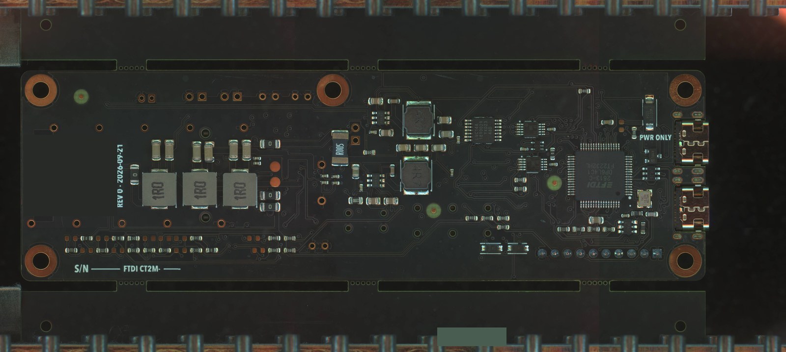
A real rev 0 board, bottom side, in JLC's production photo: the FT2232H, the two buck convertors, the three module-rail inductors and the 5 mΩ shunt. Part 5 shows both sides as they arrived.
As Part 1 explained, the MINI started life as a footprint coupon for a bigger board. It has no MCU, no firmware and no telemetry ADCs, and the brief I wrote for it says so in one line: “If a feature needs firmware, it does not belong on the coupon.”
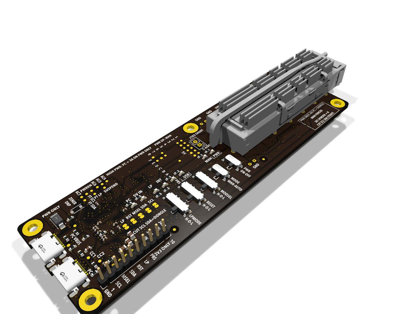
The top side render. The slide switches give a human the control lines (MODSEL, RESET, LPMODE as High/Open/Low) when no PC is attached, and the silk explains every strap and pin.
data + 5 V"] PW["USB-C 'PWR ONLY'
5 V charger, 3 A"] subgraph POWER["power"] Q["AO3401A
charger-wins switch"] --> D1["Schottky diode (SS54)"] D2["Schottky diode (SS54)"] D1 --> SYS(["VBUS_SYS"]) D2 --> SYS SYS --> BL["AP63203
+3V3L logic"] SYS --> BM["AP63203
+3V3_MOD module rail"] SWP["SW_PWR"] -. "EN" .-> BM BM --> SH["5 mΩ shunt
+ injection link"] --> FIL["3 × 1 µH filters
VccRx / VccTx / Vcc1"] end subgraph CTRL["management and control"] ESD["USBLC6-2 ESD"] --> FT["FT2232H
channel A in MPSSE"] FT --- EE["93LC56B EEPROM
USB config + FRU"] IL["interlock
no PC = MANUAL"] SWM["SW_MODE AUTO / MAN"] --> IL HOL["H-O-L slides"] --> OVR["TS5A23157
override switches"] FT -- "ModSelL / ResetL / LPMode" --> OVR IL --> OVR OVR --> STR["cuttable straps
+ 1x10 debug header"] FT -- "SCL / SDA" --> STR end PC -- "VBUS" --> Q PW -- "VBUS" --> D2 PC -- "D+ / D-" --> ESD PC -. "VBUS_DET" .-> IL STR --> CAGE["QSFP-DD connector + press-fit cage"] FIL --> CAGE CAGE -- "ModPrsL / IntL" --> FT CAGE -- "PRS / INT / LP" --> BUF["74LVC14 buffers"] --> LED["status LEDs
under light pipes"]
Power comes in through two USB-C ports. PC carries data and 5V from the laptop, and PWR ONLY takes a charger that advertises 3A. Two SS54 Schottky diodes OR them into one rail, and a P-FET turns the PC path off whenever a charger is on PWR ONLY, so the laptop never shares the module load with a charger. With no charger, the PC port feeds VBUS_SYS on its own.
For a human with no laptop around, two TS5A23157 analog switches pick, per control line, between the FTDI and a High/Open/Low slide switch, and a gate forces the slides whenever the PC port is dead, so a floating FTDI can never drive the module. The five host-driven lines also pass through cuttable solder straps next to the one 1x10 debug header, and cutting the SCL and SDA straps hands the bus over to any 3.3V I2C dongle.
Eight LEDs report all of this. PWR, MAN, USB (laptop 5V present), PRS, INT and LP sit in a row, and 5V IN (charger present) and PC (FTDI configured) sit at the rear. (btw, I/Agents screwed up the LED brightness and some of them are blinding, expecially when working on the board in the middle of the night in a dark room. )
| Part | Job | Why this one |
|---|---|---|
FT2232H |
USB to I2C and GPIO | MPSSE gives an I2C master and GPIO with no firmware, pyftdi drives it from Python, and it is the same chip and pin map the big board uses |
93LC56B |
FTDI configuration EEPROM | the FTDI’s own companion part; its spare bytes hold the board’s field-replaceable unit (FRU) record |
AP63203 (x2) |
5V to 3.3V bucks |
2A, fixed 3.3V, a small six-pin package; one per rail so the module rail switches without touching the logic |
TS5A23157 (x2) |
AUTO/MAN override | a dual SPDT analog switch passes either source to the pin without caring about direction |
74LVC14 |
LED drivers and the interlock inverter | six Schmitt inverters drive the LEDs so no LED loads a module pin |
USBLC6-2 |
USB ESD | the usual low-capacitance clamp on D+ and D- |
SS54 |
diode-OR of the two inputs | 5A Schottky, with margin at the 1.6A input current the board draws at 6W, in exchange for heat |
AO3401A |
charger-wins switch | a P-FET whose gate comes from the charger input |
The module rail itself goes through a 5mΩ shunt, a 0Ω link where a bench supply can be injected, and the three-group LC filter that the QSFP-DD MSA (the multi-source agreement that defines the form factor) asks for, with one 1µH group each for VccRx, VccTx and Vcc1. Every module-side pull-up hangs off that filtered rail. The connector is an Amphenol SMT part that JLC placed, and the press-fit cage goes over it by hand.
3.1 Power and heat set the limits
The 2A module buck sets the power ceiling. A QSFP-DD module advertises a power class in page 00h, and the MSA (Rev 7.1, Table 12) ties each class to a maximum. Class 1 is 1.5W, class 2 is 3.5W, class 3 is 7.0W and class 4 is 8.0W, all at 3.3V within 3.135 - 3.465V. Two amps at 3.3V is 6.6W, which is the buck’s nominal ceiling, and at the low end of the tolerance, 3.135V, those 6.6W already need 2.1A. That is one more reason the default budget is lower. The tool checks each module’s power against a software budget, 6W by default. The figure it checks is the larger of the advertised maximum and the lower bound of the declared class, so a module can’t slip in by under-reporting, and every class 4 to 8 module is refused. The Credo AEC, class 3 at 4.5W, fits easily. The MSA also lets a class 3 module draw a 2.8A peak for up to 50 µs at power-up (Table 13), and the design notes argue on paper that the rail’s output capacitors can carry it.
I have to own up to something here, in the order it happened, and please don’t copy it. When I ran the optics in Part 5, the budget was a software value I could raise, and I raised it on purpose from the 6W default to 8.5W so that modules advertising 8W would be let in. That was a deliberate out-of-rating characterisation of a research build. I never read the shunt during those runs, and the only thing watched was the module’s temperature, not the buck or the diodes. The 0.3.0 release closed that door after those runs. The budget now stops at 6.6W, and an 8W module is refused.
Every watt at 3.3V comes from 5V USB-C through a diode and a buck. At 6W into the module the board draws about 1.6A from the charger, and with the Schottky dropping about 0.4V, the diode alone dissipates roughly 0.7W. That’s why the board wants a charger on its own port, and why the diodes got a copper rule of their own (below).
Nearly all of that power turns into heat inside a module the size of a stick of gum, and it leaves mainly through the cage and its heat sink. On a bare board with no airflow, the AEC settled near 50°C, while an 8W-class optic kept climbing until the CMIS set throttle stopped it, and a desk fan on the cages changed that picture completely (Part 5 has the plots). So the software pulls LPMode high at 70 °C (or at 5 °C below the module’s own high-temperature alarm, if that is lower), and the next revision designs a fan in. The agents had already seen this coming in simulation, before the boards existed.
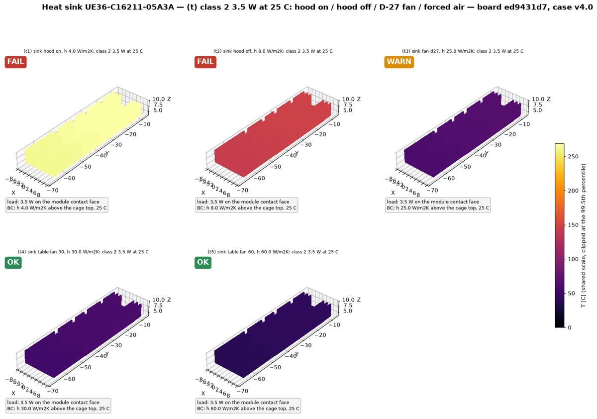
One of the thermal simulation sheets the agents generated for the heat sink: hood on, hood off (the hood is the case's cover over the cage), fan and forced air at 3.5 W. The red FAIL tile is the closed hood, and the bench later agreed with it.
The thermal sheet above is a simulation, not a measurement. An agent took the heat sink from the cage maker’s STEP model, meshed it with Gmsh, and solved steady heat conduction with scikit-fem, an open-source Python finite-element library. The module puts 3.5W into the sink’s contact face, and the air takes it off the fins through one heat-transfer coefficient per case: 4 W/m²K with the hood closed, 8 open, 25 with a small fan and 30 to 60 with a desk fan. Those coefficients come from textbook convection formulas, not from a test, so the agents marked every one of them as an assumption to check on the bench. The model also ignores the heat that leaves through the board, which makes it pessimistic. Part 4 lists the same tools for the case’s stress and drop checks, and Part 5 has the temperatures the bench measured.
3.2 Live component data
The very first surprise came before the kickoff. The parts list I started from, were full of “well-known” JLC Basic numbers. The comonnent engineer agent checked them against the live LCSC pages, and three of the popular ones were wrong. One “0Ω” link was actually a 1kΩ resistor, and two ICs had their stock collapse to single digits. My instruction after that was short: “I want data to be verified against live JLC data and not some cached info.”. This goes to teh skill as well.
From then on, no LCSC number went into the BOM unless an agent had fetched its page in that session and recorded the date, URL, stock and Basic or Extended status. Before the order, all 61 codes on the MINI were re-fetched one at a time, and none came back not found. A stock gate also wanted every line to cover the five boards in the order plus 20 %, and at least 1,000 on the shelf for the FT2232H and the analog switch. (Stock levels moved between checks, so the margin was there for a reason.) The case hardware later got the same routine, read from DigiKey Canada’s product API, with exact part-number matches only.
Datasheets got the same treatment. Before a part is drawn, an agent reads its primary datasheet and writes a note that cites the page and section for every number it uses. One of those notes caught the SS54 diodes. Their 60 °C/W thermal resistance assumes 5 × 5 cm copper pads, which a 42 mm board can’t give them. The layout rule that came out of it is at least 150 mm² of cathode copper per diode, stitched by six or more vias to the same VBUS_SYS pours on the other layers, including an island on In2 (the second inner layer). That only closes part of the gap, so the diodes stay the hottest parts after the module and rev 1 replaces them.
Some inputs still needed my hands. The Amphenol connector and cage drawings and 3D models sit behind a sign-in and a licence, so I downloaded those myself. The agents took every footprint dimension from them and keep the files in a folder that never leaves the private repository. Each time, the agent wrote down exactly which file it needed and why, I fetched it, and the agent recorded where it came from. Provenance is key to reproducibility, and I had to reenforce that lesson a few times before the agents got it.
4. Where everything goes: the placement decisions
Most of the board’s character was settled during placement. The case and the cable conector positioning fixed the big parts, and everything else followed from them, roughly in this order. This section covers why each part sits where it does. How the placement itself is made, as a CSV file of positions and a script that applies it, is in Part 3, section 2.2, together with the layout and the routing.
From the start, the plan was a 3D-printed case, so the board had to fit a printed shell. Part 1 shows two finished units in their printed cases, and Part 4 tells how the case was made. The photo below shows two of them on the bench.
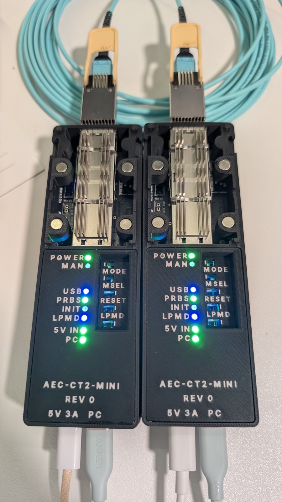
Two rev 0 units in their printed cases, the same pair as in Part 1. The cage nose forms the front bezel, the LED labels and light pipes run in one line on the lid, and the switches sit in one slot beside them.
My original plan was a 70 × 100 mm board with every part on top, and it didn’t survive the case. A 42 × 136 mm stick, about twice the width of the cage, made the case, the two-unit coupling and handling on the bench far simpler, so the form factor changed before any routing started. That changed the rule about parts too, since a 42 mm board can’t hold everything on one side. The cage, switches, LEDs, the debug header and the test points live on top, and almost all the ICs live underneath, below the areas of the top that carry no through-hole pins.
The cable connector and cage decided the front edge. The cage is press-fit, its nose becomes the bezel of the case, and a heavy cable pulls on it, so the cage gets the front edge to itself, with nothing else within 10 mm and only ground copper under it. Five M3 holes, one in each corner and one just behind the cage, send the plug’s torque into the case through screws rather than through the press-fit joint. Both USB-C receptacles went on the rear edge, mid-mount in board notches, so the plug axis sits level with the board and the case needs only one low window.
On the top side, the case had the final say. One row of slide switches with the LEDs next to it means one slot bar and one line of light pipes in the lid. (Six LEDs share that line, while the 5V IN and PC LEDs at the rear sit slightly off it, which rev 1 fixes.) Those positions went straight into the case model and into a printed dummy board.
The electronics then filled in around those fixed points:
| Constraint | Choice | Why |
|---|---|---|
| Power enters at the rear | Diode-OR, charger-wins switch and USB ESD clamp at the receptacles, diodes out of the heat sink’s shadow | The USB data clamp is the first thing a D+/D- surge meets, and the diodes are the hottest parts after the module |
| The bucks need full width and short hot loops | Both bucks just behind the cage, input capacitors at the VIN pins, inductors beside them |
Behind the cage is the first place where the full 42mm width is free, and the switching loop stays inside a few millimetres |
| The module rail must be quiet at the connector | Shunt and injection link behind the cage, the three LC filter groups directly under the connector’s power pads | Each filter group ends a few millimetres from the pads it feeds, and the shunt sits where a meter can reach it |
| The FTDI talks to USB and to the module | FT2232H near the USB-C ports, crystal and EEPROM beside it |
A short USB pair, and the FTDI drives the module pins directly with no I/O expanders |
| Decoupling only works at the pin | Every decoupling capacitor within 2.5 mm of its pin |
The placement checker refuses the board otherwise |
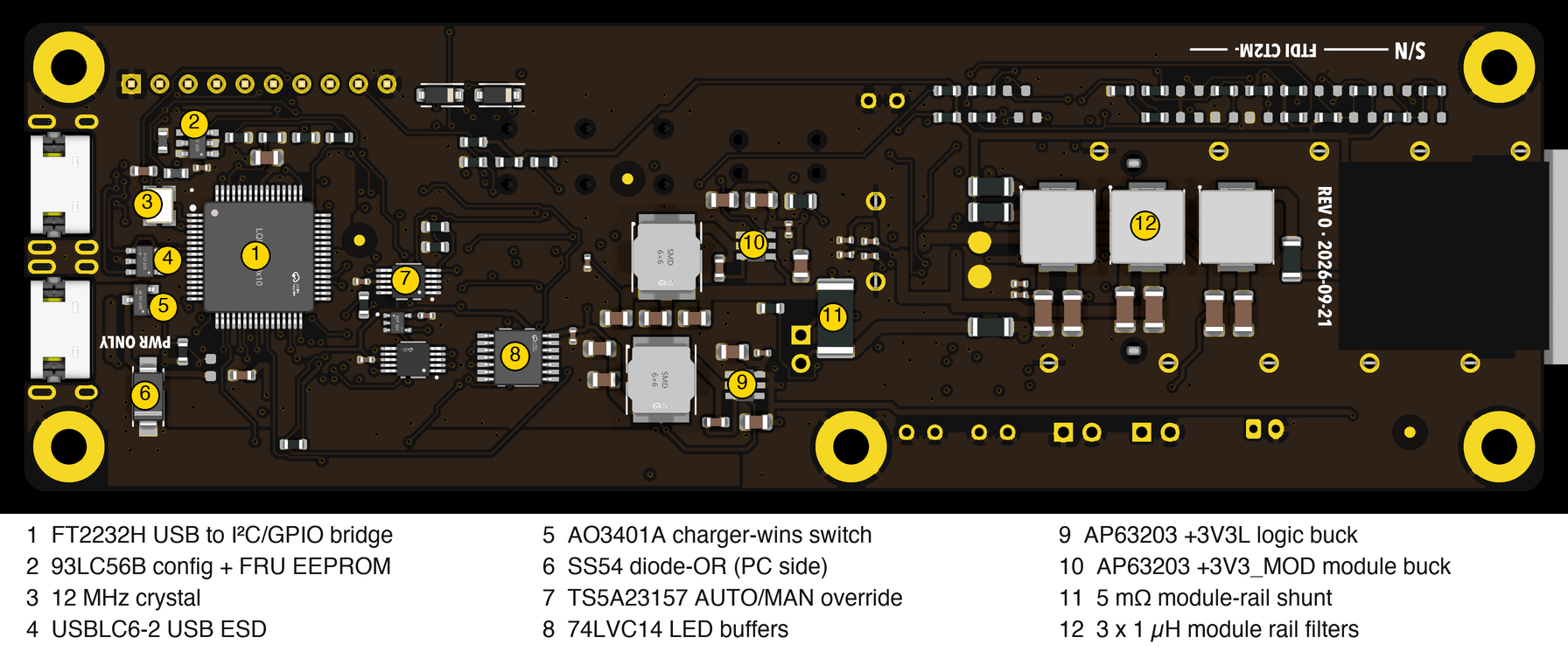
The bottom side, rear USB-C edge on the left, the cage end on the right (the cage is on the other side). The numbers follow the placement order: protection at the rear, the FTDI near USB, the bucks behind the cage, the filters under the connector pads.
The reviews moved some parts and argued about others. The analog override switches moved once, off a power-plane corridor they were pinching, which also gave the routing a cleaner channel. Reviewers also asked for three changes that needed a different outline or more room. They were un-stacking the two diodes from a shared copper area, widening the thin rib between the two USB-C notches, and moving the switch row about 4 mm to make room for the cage’s own light pipe (the cage ships with one beside the port). None of them was worth re-routing rev 0 for, so each one became a rev 1 requirement with its reason written down.
What is and isn’t proven: the class table, the CMIS map and the placement are design facts. The 6.6W ceiling comes from the buck’s arithmetic and was never load-tested, the inrush is only argued on paper, and the 8W runs were out of rating.
Previous: Part 1: what it does and what it found. Next: Part 3: the design flow and making it: schematics from YAML, the waivers, replayable placement and routing, the layout and JLC’s checks.


Leave a comment